
When a defect might be beneficial
Making strides toward improving semiconductors for solar cells, LEDs
In the quest to design more efficient solar cells and light-emitting diodes (LEDs), a team of engineers has analyzed different types of defects in the semiconductor material that enables such devices to determine if and how they affect performance.
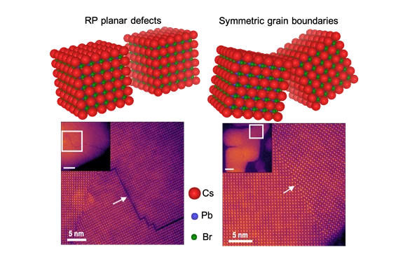
Rohan Mishra, assistant professor of mechanical engineering & materials science in the School of Engineering & Applied Science at Washington University in St. Louis, led a team of researchers at WashU, at Oak Ridge National Laboratory in Tennessee and at the University of Missouri-Columbia that studied the structure and properties of the commonly occurring planar defects at the atomic scale, which spans only a few tenths of a nanometer.
Mishra's team studied lead-halide perovskites, a new class of high-performance semiconductors that are being explored for the next-generation of low-cost solar cells to enable conversion of solar energy into electricity with high efficiency. When these materials are made, defects can occur where different crystals meet, known as grain boundaries. In conventional semiconductors, these defects can decrease their electrical conductivity and the solar energy-to-electricity conversion efficiency; however, in lead-halide perovskites, there are differing experimental reports on the activity of grain boundaries. In some cases, they are found to be harmful, while in other cases they either have no impact on performance or are even beneficial, but to date, no one understood why. Mishra's team explained why in Advanced Materials Dec. 3.
"A tiny defect at the atomic scale has a big impact on the solar cell," Mishra said. "If one specific atom is missing at these grain boundaries, your cell won't work well."
At Oak Ridge National Lab, Arashdeep Singh Thind, a doctoral student in Washington University's Institute of Materials Science & Engineering who works in Mishra's lab, performed the imaging with one of the most powerful electron microscopes to look at the atomic structure of the grain boundaries. Guangfu Luo, a former research scientist in Mishra's lab who is now an assistant professor at Southern University of Science and Technology in Shenzen, China, then used quantum-mechanical calculations performed on some of the fastest supercomputers to understand the electronic properties of these grain boundaries.
"By using this combination of microscopy and theory, we are able to not just understand the structure, but also the electronic properties," Mishra said. "If we understand them, we can engineer better materials with improved properties. So far, no one had been able to observe this, but now we can."
In silicon semiconductors, grain boundaries wreak havoc, but in lead-halide perovskites, they may not, and that depends on concentration of the halide ions, a critical element to the properties.
"If you grow the crystals in a halide-poor environment, then the grain boundaries are terrible for performance," Mishra said. "But if you can grow them or anneal them in a halide-rich atmosphere, the grain boundaries are fine."
Thind also looked at another type of planar fault known as Ruddlesden-Popper faults, in which the planes of crystals stack incorrectly; for example, instead of being lined up in neat rows, one of the rows is shifted slightly left or right by an atomic column. Again, by using quantum mechanical calculations, Luo and Mishra found that by having a large density of such stacking faults, it might be possible to obtain bright optical emission from large and more stable nanoparticles of certain lead-halide perovskites, which could potentially pave the way for LEDs with longer lifetime.
"The challenge for experimentalists is to engineer stacking faults at periodic distances," Mishra said.
In related research published in ACS Applied Nano Materials Oct. 16, Mishra's team worked with the researchers at the University of Missouri-Columbia who found a new chemical route for promoting growth of lead-halide perovskites with a high density of such stacking faults. By removing surface ligands, an ion or molecule that binds to a surface atom of a nanocrystal, smaller lead-halide perovskite nanocrystals fused and grew from about 8 nanometers to 60 nanometers in 48 hours.
These new nanocrystals had significantly enhanced optical properties due to the stacking faults formed during the fusion process, which Thind found using atomic resolution scanning transmission electron microscopy. In addition, the nanocrystals were more stable when exposed to light, had sharper emission lines and a higher quantum yield. With these defects, the new nanocrystals are expected to improve light emission properties of the lead-halide perovskite nanocrystals, resulting in better LEDs and other optoelectronic devices.
This new information gives engineers such as Mishra and Thind more information to find alternatives for lead in solar cells, which not only contain toxic lead, but also are unstable in light, moisture and heat and break down in a matter of days, leaking lead into groundwater. Mishra is studying whether a nontoxic element — bismuth, lead's neighbor on the periodic table — is a safer and equally efficient substitute for lead in perovskites.
Thind A, Luo G, Hachtel J, Morrell M, Cho S, Borisevich A, Idrobo J-C, Xing Y, Mishra R. Atomic Structure and Electrical Activity of Grain Boundaries and Ruddlesden-Popper Faults in Cesium Lead Bromide Perovskite. Advanced Materials. Dec. 3, 2018. DOI: 10.1002/adma.201805047
This study was funded by the Ralph E. Powe Junior Faculty Enhancement Award from Oak Ridge Associated University and the National Science Foundation (DMR-1806147).
Morrell M, He X, Luo G, Thind A, White T, Hachtel J, Borisevic A, Idrobo J-C, Mishra R, Xing Y. Significantly Enhanced Emission Stability of CsPbBr3 Nanocrystals via Chemically Induced Fusion Growth for Optoelectronic Devices. Applied Nano Materials. Published online Oct. 16, 2018. DOI: 10.1021/acsanm.8b01298
Click on the topics below for more stories in those areas
Back to NewsFaculty in this story


